
![]()
|
|
|
|
|
|
Intusoft Newsletter Issue
#57, September 1999
Copyright ©2002
Intusoft, All Rights Reserved
| In This Issue | |||
| 1 | Control Loops/Emitter Follower | 4 | Magnetics Designer 4.1.0 |
| 2 | Singing Filters | 5 | ICAP/4 version 8.x.7 and Scope5 Beta |
| 3 | Filtering Ground Loop Noise | . | . |
Designing a stable control loop can be a black art. When multiple loop systems are encountered, application of the basic principals for stability analysis often fails to identify a marginal circuit design. Small component variations can cause large changes in gain and phase margin when the wrong control loop is chosen to measure gain and phase margin. As we discussed in our last newsletter, the open loop frequency response of a system can be measured with the loop closed, simply by inserting an AC generator in series with the signal flow. The freedom to easily select a place in the signal flow to “cut” the loop leads to many different views of control system stability. Finding the proper place to measure the open loop response can be a formidable problem for multi-loop circuits.
This article begins with the “intrinsic” feedback
loop of an emitter follower. Then it delves into the mysterious
multi-loop problem of the singing input filter of a switched mode
power supply.
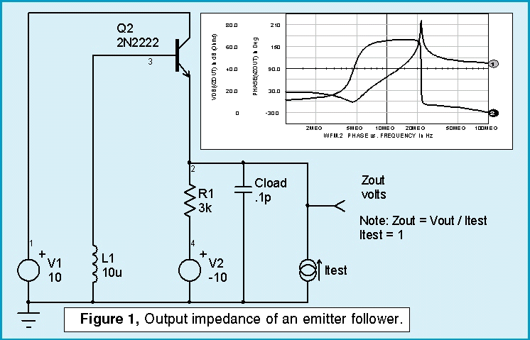
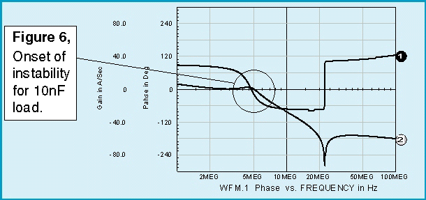
To begin with, an emitter follower becomes unstable with inductive base impedance because the transistor’s beta rotates the base impedance vector as beta falls off with frequency, thereby exposing a negative resistance at the emitter terminal. A capacitive load can form a resonant circuit with negative damping and therefore cause oscillations. Figure 1 illustrates the effect from an impedance point of view. In this circuit, from inspection, a capacitive termination ranging of 10 nF at 5 MegHz to 8 pF at 20 MegHz will result in exposing the negative real part of zout. This results in oscillation.
Side BarThese numbers are calculated based on the impedance as seen
in the graph when the phase is greater than 90 degrees. This
occurs between 5MegHz and 20MegHz. At 5 MegHz, the magnitude
is 10.8 dB or about 3 ohms. Then |
But where did the inductor come from? Base inductance can occur most commonly from long wires; for example, clip leads or test equipment wire harnesses, or from the circuit which is used to drive the emitter follower. Adding an emitter follower to an op-amp output or using Darlington connections are common circuits that add base inductance.
Control system stability is expressed in terms of gain and phase margin. In order to apply the theory, a control loop must be identified. The “intrinsic” feedback of an emitter follower doesn’t lend itself to this method because there is no control loop to be found. We can, however, make a model of the transistor that allows an “intrinsic” loop cut to be made within the device. Having established a valid control loop within the device, the stability criteria can be compared with several external loop cuts.
The output impedance (shown in Figure 2) using the intrinsic transistor model is similar to that which was measured in Figure 1. It would be best to use the detailed Spice model for the final result because the model automatically accounts for changing bandwidth as a function of operating point. The reason for exploring the intrinsic feedback is to find an external loop that gives decent results so that it is unnecessary to manually account for the internal transistor behavior.
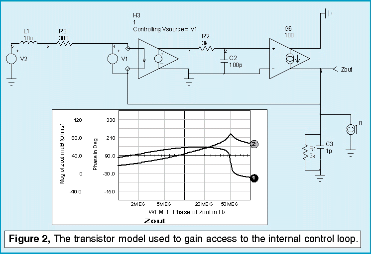
The circuit which is used to model the transistor is highly simplified when compared to the Spice model. What we want to determine from this model is whether or not external control loop cuts can provide reasonably accurate values for gain and phase margin.
 |
A loop cut is made by inserting a series AC source and identifying Vout as the input side of the source and Vin as the output side. Input and output are identified as the signal flow direction. If you reverse them, the gain and phase going backwards will indicate that they should be reversed. Making loop cuts in this manner allows the simulator to solve the DC operating points without concern for AC stability, basically performing the open loop analysis on a closed loop circuit. The technique works much better in a computer simulation than for real hardware, because the circuit can still be observed when it’s unstable. Figure 3 shows the gain and phase, along with the intrinsic loop configuration. |
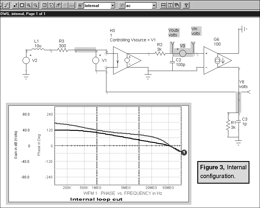 |
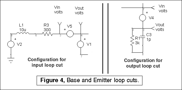
Next, the control loop is cut at the base and at the emitter, as shown in Figure 4. These configurations were easily generated using ICAP/4’s configurable schematics feature. Each configuration has its private topology on a separate layer. The main portion of the drawing is on another layer. The configurable feature of the schematic allows different drawings to be made by combining different layers as needed. In this case, there were 4 drawings; “zout”, “internal”, “input“ and “output.” They all share the same components, with different Spice generators and test points. The components used specifically in the “internal” configuration are the shaded objects which are shown in Figure 3.
Simulation results for each of the configurations are shown in Figure 5, below.
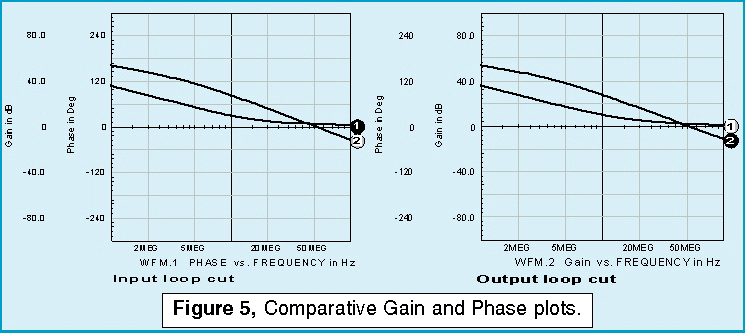
The onset of instability is predicted using the cut at the emitter
and the cut at the base. Given the inaccuracy in modeling the
transistor, the external loop cuts provide reasonably good results,
based on classical control system theory. Finally, the original
circuit stability prediction using a loop cut at the emitter (Figure 1) yields the results shown in Figure
6.
For additional information, see Intusoft Newsletter #56, SideBar:Obtaining open loop gain and phase characteristics using a closed loop test.
An efficient power supply conserves power so that its output power is the input power times the efficiency:
Iin x Vin x Efficiency = Iout x Vout
Taking unity as the limit for Efficiency and letting the regulator vary the duty ratio to make Iout*Vout constant, then
d(Iin x Vin) = 0 = Iin x dVin
+ Vin x dIin
Solving for Rin yields
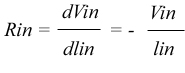
The small signal equivalent circuit of a switching power supply
is then a negative resistor!
Needless to say, many passive filters oscillate (also called “singing” if it oscillates at a frequency within the audio frequency range) when they’re connected to a negative resistance load. Even worse, the input filter could itself be a switching power supply belonging to a test set or a facility power factor correcting circuit. So we face a dilemma: whose circuit is oscillating?
To answer the stability question, the power system must be considered as one entity. Credit or blame for the result falls in the domain of electro-politics, a topic for another day. First, a model is needed in order to explore the stability problem. The input and output filters and the control amplifier are handled easily, using standard IsSpice models for resistors, capacitors, inductors and operational amplifiers. The nonlinear or switching portion is well characterized using an averaged model for the pulse width modulator.
Rather than using an IC PWM, we will use this average model from the ICAP/4 Part Browser, along with a generic op-amp for stability compensation in order to draw attention to the stability issues in the control system. Figure 7 illustrates the state average model for the power supply.
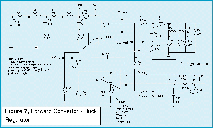
The control loop consists of an inner current sensing loop with an outer voltage control loop. Integrating the voltage across the buck regulators filter inductor will sense the current. An integrator is needed for the voltage control loop, so the same integrator does double duty. This method of obtaining current feedback skirts the noise issue found in schemes that use resistors to sense current. Performing the integration requires the integrator to be configured as a differential device. C9, R12, C10, R18 and C12 are used to form the differential connection. Connecting node 7 to node 27 activates the differential components in order to find their affect on performance.
The input filter is a conventional 2-stage EMI filter. As in most power circuits, the performance is determined by parasitic components. The main culprit is capacitor ESR. R8 is used as a damping element that stabilizes the EMI filter – PWM interface.
There are 5 configurations used to test different control loop
cuts for stability. The one shown makes the loop cut between the
EMI filter and the pulse width modulator. The other cuts are at
the PWM control point, the Buck Regulator filter, the current
loop input, and the voltage loop input.
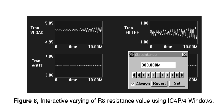
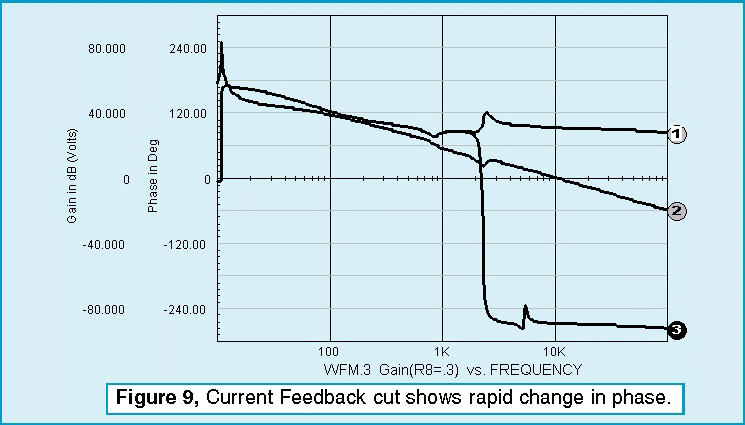
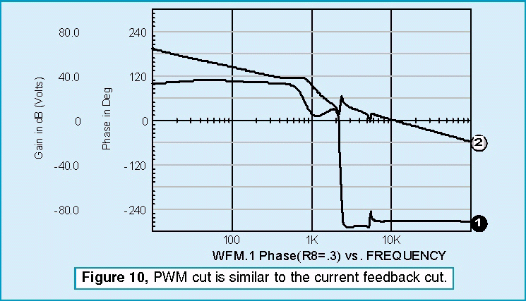
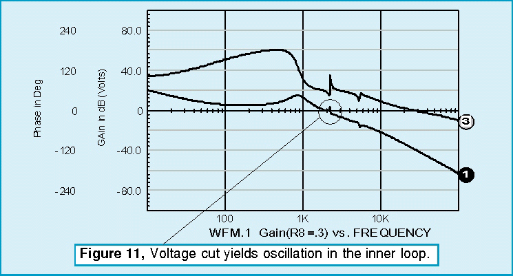
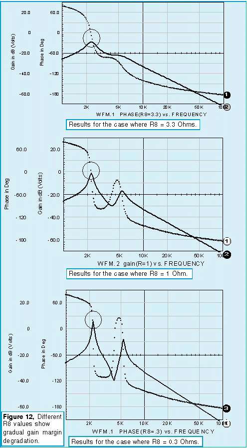
The only loop that needs additional components is the current feedback loop. Leaving the outer voltage loop inplace produces an undesirable interaction at low frequencies. To block the outer loop, a large inductor is inserted in series with the voltage feedback. All loop cuts except the one shown produce a sudden onset of instability as the zeros caused by the input filter move from the left-half of the complex plane to the right-half plane. Recall from root locus theory that the closed loop poles migrate toward the open loop zeros. Right-half plane zeros will then “pull” closed loop poles into the right-half plane, thus causing oscillation. From a topological view, right-half plane zeros arise in multi-loop systems because a difference in polynomial ratio transfer functions takes place. This results in negative numerator roots. This difference occurs in the pulse width modulator if you break down the small signal current and voltage transfer functions. By placing the loop cut at the input to the PWM element, the right-half plane zeros are eliminated from the open loop response, and we see a more gradual loss of stability as the gain at the cut point approaches unity (Figure 10). The voltage loop seems oblivious to the instability. That’s because oscillation is occurring in the inner loop; the poles seen by the voltage loop have already migrated to the right half plane and the bode plot isn’t showing the singularity because the exact frequency wasn’t selected for the analysis (Figure 11). For those who like to tweak critical components and watch the instability grow, the interactive features of IsSpice allow those endeavors. Figure 8 shows the interactive capability varying R8 and viewing the onset of oscillation in a transient simulation. Figure 12 shows the results for three different values.
Ground loop noise is caused by the coupling of the AC mains return to the chassis or local PWB ground through stray capacitance. The switching transistor in a switched mode power supply generates the noise. The schematic in Figure 13 illustrates the noise path.
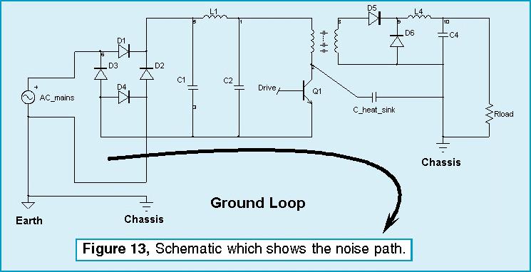
The rectifier bridge alternately connects one side or the other of C1 to ground when the diodes conduct; otherwise the connection is through the diode stray capacitance. The diode bridge switching is very slow compared to the switching frequency of Q1 so that a simplified model can be made for each of the non-linear regions presented by the bridge rectifier. The lowest impedance coupling occurs when the bridge diodes are conducting; so a simplified worst-case model replaces the AC signal with its peak rectified DC counterpart. Both 3-wire and 2-wire AC distribution systems are in wide use. For this problem a 2-wire system will be modeled. We will place a series inductor and resistor in the ground leg between the power supply and the AC ground. The AC ground will then be connected to our chassis to complete the ground loop.
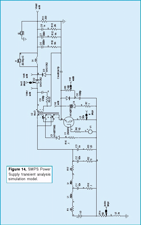
Noise is coupled into the circuit through the stray capacitance between the switching transistor and its heat sink and through the inter-winding capacitance of the forward converter’s transformer. In order to measure the noise, we will use a forward converter design that isbeing prepared for a future article featuring a complete power supply design using our Power Supply Designer package. The transient analysis model for the power supply is shown in Figure 14.
Magnetic Designer 4.1.0 was used to design a sector wound transformer with very low primary-to-secondary coupling capacitance. Most coupling comes from the power transistor to heat sink path. The heat sink could be isolated or connected directly to the chassis. Using a coupling of 5pf for an isolated heat sink .vs. 50 pf using the chassis results in the noise shown in Figure 15.
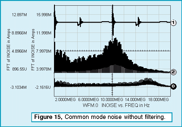
Taking the FFT of the transient response presents the data in a form that can be compared with various EMI specifications. MIL-STD-461D allows for the following conduced interference:
CE101
CE102
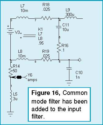
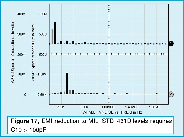
The inductive nature of the power line makes CE102 more difficult; in any event, the power supply is badly out of spec. Common mode filtering is needed to solve the problem. If L1, the 300uH inductor in the first stage of the input filter, is replaced with a coupled inductor that has high common mode impedance, that will provide the differential filtering we need. There should also be a return path (provided by C10) for the noise within the power supply. This capacitor comes with certain disadvantages. It connects the emitter of the switching transistor to the chassis. If the chassis weren’t grounded to the safety ground, then the chassis would be electrified by a combination of the 100KHz switching signal and the 60Hz power as seen across the bridge rectifier. Neither of the voltage sources is hazardous to people because the impedance is high; however, they could provide sufficient energy to damage MOS interface circuitry. It turns out that making C10 as little as 100pF is adequate, and may prove to be a good compromise.
Different applications will face a variety of power and signal line impedances and connectivity. You should explore each of these in order to make your design decisions. We have covered only one example of many possible design configurations.
Magnetics Designer version 4.1.0 began shipping on Sept. 1. It
contains many powerful feature additions (http://www.intusoft.com/Mag.htm).
The files for this version will be posted on our technical support
page throughout September. Version 3.1.1 users who have current
maintenance can either download verion 4.1.0 from our web site,
or wait for the CD to arrive automatically.
BACK
TO THE TOP
ICAP/4 version 8.x.7 will be released in the 4th quarter... and the Scope5 beta version will be posted on our web site in September.
Copyright ©2002 Intusoft, All Rights Reserved