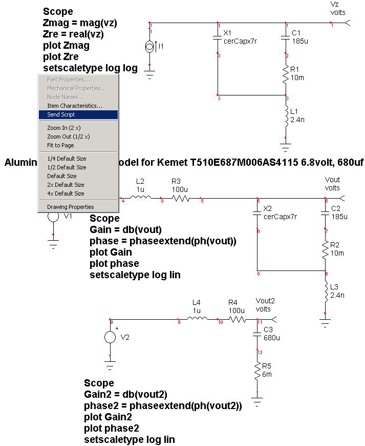
|
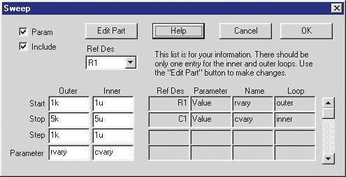
Easily Add Sweep and Optimize Part
Parameters — Within Sweep and Optimize dialogs you can now select
from a part list and edit part parameters without leaving the dialog
box.
|
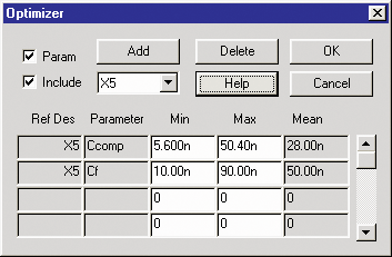
Better Optimizer Information — After
you enter a percent tolerance for the optimized parameter, you
are able to view the minimum, maximum and mean value for that
parameter.
|
 |
Modified B Element — Added the capability to
copy “B Element” expressions to the part comments, so they will be displayed
on the drawing. An Enter dialog was added for ease of entering very
long expressions.
New ICL Scripts Added — Expandx, expandy,
and expandxAllPlots ICL scripts were added to let you easily modify
your waveform viewing area. Family script was added to create eye diagrams.
Superfamily script combines multiple vector tags into one to reduce
presentation clutter. Drawing scripts allow you to easily format waveform
graphs.
Easy Location of Subcircuit Vectors — The Add Waveform Dialog
in IntuScope now features an expandable tree structure for subcircuit
vectors.
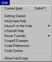
Dynamic Help Menu For Scope5 —
HELP now includes updated Movie Tutorials, and web access to the
latest documentation.
|
|
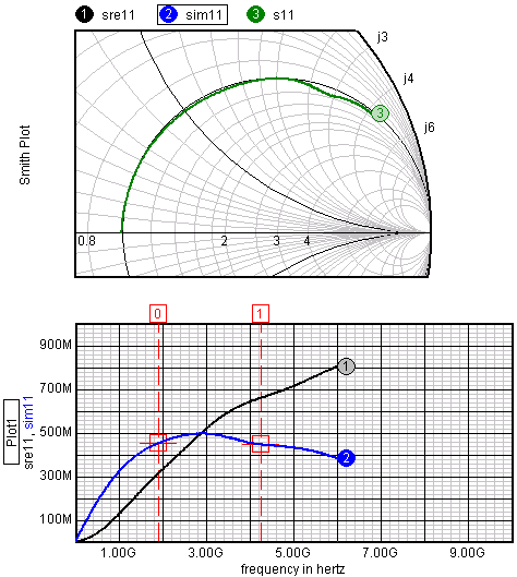 |
Smith Charts — As
a Test Designer, ICAP/4 Professional, or RF user, you can now plot
Smith Charts by reading in a Touchstone formatted file. Smith Charts
may be used to calculate impedance determination, impedance matching,
noise figure optimization, or stability.
|
The forward converter Z-Transform model extends the approach
used by Yaakov [1] in which behavioral relationships were directly implemented.
Rydley [2] demonstrated the need for modeling transport delay. However,
in this case, a Z-Transform model implements this affect directly. Various
loss mechanisms can be added to the large signal model in order to predict
DC-DC converter efficiency using an operating point analysis. The following
model elements will be discussed and the behavioral equations developed.
| Table 1.
Efficiency Measurement
|
| Rload |
Pload |
From OP Analyses |
From TRAN Analyses |
| .2 |
125 |
62.5% |
62.7% (Ron set to match) |
| .7 |
37.5 |
81.8% |
81.8% |
| 1 |
25.0 |
84.6% |
84.4% |
| 2 |
12.5 |
88.1 |
87.8 |
| 4.7 |
5.3 |
89.5% |
89.5% |
| 10 |
2.5 |
88.6% |
88.8% |
| 20 |
1.25 |
85.6% |
87.2% |
Model
Elements
1. Sampling theory
2. CM/VM Control law
3. Fraction Order Hold
4. Z Transform Integrator
5. CCM/DCM mode switching
6. Input and Output current/voltage equations
7. Magnetizing inductance effects
8. Leakage inductance induced losses
9. Transistor switching loss
10. Switched capacitor loss model
11. Resistive Losses
12. Core Loss
Sampling
Theory
To achieve a large signal model, the cycle-by-cycle
switching difference equation must be derived. It is not suitable to
assume conservation of power through the converter at each instant because
the reactive elements store and release energy. Z-Transform theory predicts
the time domain performance at each sampling instant. For the class
of PWM circuits, it is convenient to set this instant at the beginning
of each pulse as shown in Figure 1a and 1b. This is not very satisfying
to the end user because it under-estimates the output current. To overcome
this we calculate an average output current based on our knowledge of
the sampled data state.
Z
Transform Integrator
The waveforms for DCM and CCM are shown in Figure 1a
and 1b, respectively. We begin each cycle with the previous sample current,
I1. The calculated result at the end of the cycle, Io, is fed into the
input of the transmission line. The sample delay, Z^-1, is e^sT in continuous
time and it can be simply modeled as a transmission line. The transmission
line works for both AC and Transient analysis, thereby preserving the
small signal characteristics needed for stability analysis and also
the large signal description needed for the transient case. Idischarge
will change with the inductor conduction mode. The representation in
Figure 1c is actually a bootstrap integrator. If the gain exceeds 1.0,
the output will grow to infinity. The gain was set to .995 to prevent
numerical round off from making this circuit unstable. Reducing Gmin
increases numerical precision. As Gmin is reduced, the integrator gain
can be made to approach 1.0; however, DC convergence will eventually
fail for sufficiently small Gmin.
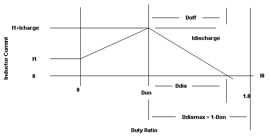
Figure 1a. The
Z-Transform sampling instant is shown at the beginning of
each pulse of this class of PWM circuits. Figure 1a shows
the waveform for DCM, where lout = Ddis*IDischarge/2.
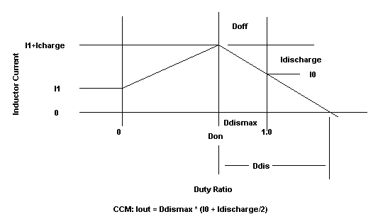
Figure 1b. The
Z-Transform sampling instant is shown at the beginning of
each pulse of this class of PWM circuits. Here the waveform
for CCM, where lout = Ddismax * (10 - Idischarge/2), is shown.
|
CCM/DCM
Mode Switching
The terms used in Figure 1a and 1b are defined as:
| Don |
The fraction of the period the switch
is ON. |
| DDIS |
The number of periods to fully discharge the inductor |
| DDISMAX |
The time available for discharge in the current period.
If Ddismax > Ddis then the mode is CCM, else its DCM. 1-2
MegHz switching Voltage Regulator Module.
|
DDIS = 1 – Don
Icharge = (Vin-Vout)*Don/(L*F)
If (Mode == CCM)
Idischarge = (I1 + Icharge)* DDISMAX / DDIS
else
Idischarge = Vout * DDIS/(L*F) |
You’ll find these equations modified slightly in the
actual model to account for snubber delay and to prevent divide by zero
during numerical iterations. Figure 2 illustrates how that was done.
Notice that the ModeCCM switch has a small hysteresis in order to prevent
numerical oscillation. You can see that variables like Don are nodes
so that the node voltage, used in the equations, becomes V(Don).
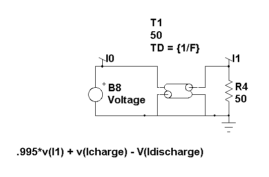
Figure 1c.
A transmission line models Z^-1.
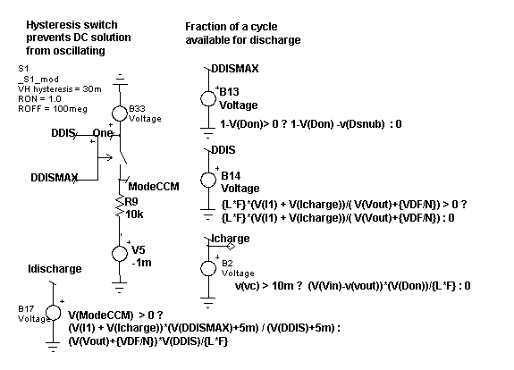
Figure 2. Calculating
average output current.
|
Output
Current/Voltage Equations
Figure 3 shows the method to calculate average output
current. These currents are sent to the output in 2 parts; charging
and discharging. The charging component (B24) is dependent on Don while
the discharging part (B4) is controlled by the mode. In both cases,
the average is taken so the output voltage and currents will be at their
average values rather than the sample data points. Diode, D2, prevents
negative output. It has a low emission coefficient, 3m, which has its
internal temperature set to 27 deg. C. independent of circuit temperature.
One of the general problems with this model is that it can find negative
solutions that have no interest. It is even possible for a positively
clamped state variable to have a negative result computed during the
matrix solution. These negative values can result in instability as
well as divide by zero overflows. That’s why you see many expressions
with positive clamped results (expression > 0 ? expression : 0).
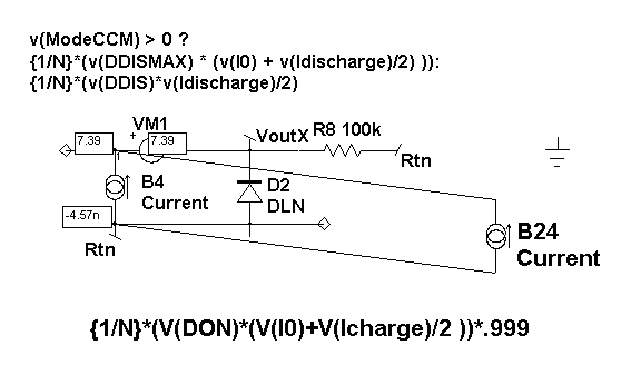
Figure 3. Equations
used to model load current, series and parallel losses.
|
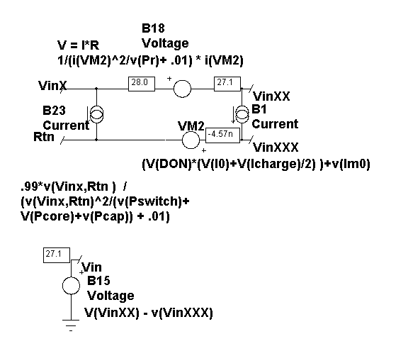
Figure 4. The input voltage
and current equations.
|
On the input side, illustrated by Figure 4, conduction
occurs only during Don. B1 computes the basic relationship. Notice the
magnetizing current, Imo, term. Its equations will be developed later
on. B23 and B18 introduce losses. B18 reduces the input voltage, simulating
resistive losses in the power switch and transformer. B23 accounts for
leakage inductor, core and switched capacitor losses. B18 and B23 are
used to model resistive and conductive losses using models that are
well behaved around zero. The following equation for B18 shows how the
parameter del prevents a singularity at zero current while squaring
the current in the denominator forces a the term to be positive, thereby
eliminating any chance for a divide by zero. Vin is referenced to simulator
ground, allowing the external inputs to be offset from ground.
V = I*R = I(VM2)*1/(1/R + del),
I^2R=P; R = P/I^2
V = I(VM2)*1/(I(VM2)^2/P + del) |
CM/VM
Control Law
The control signal, Vc, is converted from an external
ground on the input side using B10. The control signal is processed
through a fractional order hold, accounting for transport delay. This
FOH and the Z-Transform integrator realistically model the phase degradation
near one half the sampling (Nyquist) frequency.
The control equations are implemented as shown in Figure
5.
RB is the current sense resistor and the equations
assume that 1 volt will cause the maximum current flow. Setting the
parameters RB=0 and MC=1 will result in voltage mode control where the
duty cycle is set by v(Cntrl).
For CM controllers, the following
equations apply:
I1+Icharge+Imag = Vcontrol/Rb
Icharge = Don*(Vin-Vout)/(LF)
I1 + Don*Vin/(L*F) + Imag = Vcontrol/Rb
Don = (Vcontrol/Rb - I1-Imag)*(L*F)/Vin
Don = (Vcontrol - Rb(*I1-Imag))/(RB*Vin + MC)
To operate in VM set:
MC=1, RB=0
For CM MC = slope compensation as fraction of the slope |
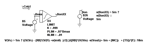
Figure 5. Control law for
both CM and VM controllers.
|
What's
*exempt all about?
We have many requests from semiconductor vendors to
increase the size limit on our demo software so that they can show how
new ICs work. The IC models and circuits have become so complex that
to increase our complexity test so these circuit simulations would run
amounts to giving our software away. In order to accommodate the showcasing
of these products, Intusoft invented a method to exempt certain portions
of a drawing from the IsSpice complexity test. This allows a simple
circuit configuration to simulate but prevents it from working when
the user adds parts and functionality needed to make a production circuit.
Here’s how it works. Right after the .subckt line in
the Spice netlist, this line is inserted in the netlist:
*exempt arg1 arg2 arg3
This causes the demo version of IsSpice to scan the
remainder of the subcircuit netlist. If the subcircuit netlist passes
the scanning test, then the subcircuit is not processed by the complexity
testing procedure. The scanning method prevents topology changes in
the subcircuit from being accepted by the simulator. Each subcircuit
is scanned according to the rules presented in its *exempt line so that
*exempt lines can’t be applied to other subcircuits.
We do this to showcase our software so that the combination
of software and models is synergistic. The whole is more valuable than
the sum of its parts, or so we hope. You will see this feature in SpiceNet
drawings from ON Semiconductor and TI in the next few months.
Intusoft recently did a Bode plot for an internal loop
model using our new Z-Transform model for the switched inductor.
The Z-Transform model shows gain greater than 1 at
harmonics of the switching frequency. This behavior suggests instability
that would fold back below the power supply Nyquist frequency.
Note: The frequencies above the Nyquist frequency are
generally taken to mean that these frequencies fold back beginning at
½ the switching frequency, extending into negative frequencies
until reversing. This behavior is well known and used in heterodyne
detection systems.
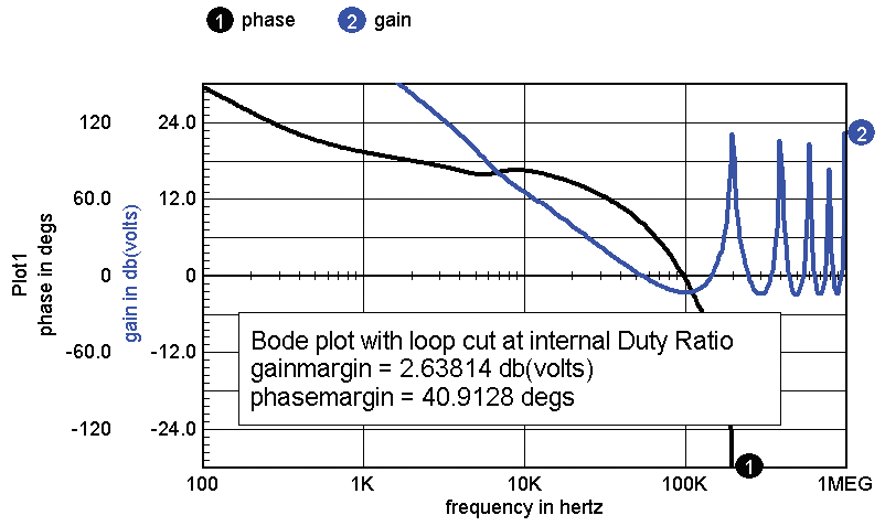
Figure 6. Bode Plot with
Loop Cut at Internal Duty Ratio.
|
There is no evidence of instability in the outer voltage
control loop, as shown in Figure 7.
The switching models transient output voltage shows
ripple primarily at the switching frequency; however, there is a small
chaotic noise component. This is shown in Figure 8.
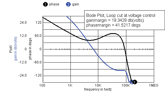
Figure 7. Bode Plot with
Loop Cut at Voltage Control.
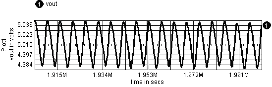
Figure 8. Switch model's
transient output voltage shows ripple at the switching frequency.
|
Questions
for Future Study
1. Is the unexpected transient ripple really there
or is this just numerical noise?
2. What is to be made of the AC response above the switching frequency?
Test Designer
Key to Structural Integrity
|
Test Designer is software which designs test strategies
to assure structural integrity. There have long been arguments over
structural versus functional testing; however, structural test MUST
be performed to assure reliability. Here’s why:
Did
You Know? You've designed redundant or fault tolerant systems
in order to ride through a single point failure. But over time it is
increasingly likely that a failure has occurred and that if undetected
a catastrophic event is likely. The availability of redundant systems
is fundamental to avoiding catastrophe. Either built in self test, BIST
or auxiliary testing is needed to perform structural testing that assures
proper component operation. This kind of testing effectively resets
the accumulated failure rate to zero for each part that passes the test.
After a successful test; then when you begin a mission, you have full
advantage of the redundant systems.
How
is it Done? It is necessary to analyze the results of each
likely component failure. Then a test strategy is necessary to detect
each fault. Work done in the USA for commercial and military aircraft
systems has produced methods for sequencing these tests to produce a
decision strategy that isolates faults. Putting this together with simulation
technology, it is possible to complete this apparently monumental task.
Say
that Again Undetected part failures make a catastrophic event
more and more likely the longer a system operates without fault diagnosis.
Fault diagnostic test design is possible today using simulation technology
and established test design techniques. That combination has been put
together with Intusoft’s Test Designer. You can even model electro-mechanical
components and perform system level diagnostic testing.
Show
me an Example Let’s try an automotive steering system. In
the near future electrical systems will replace the mechanical-hydraulic
method currently in use. The steering wheel may become something like
a force feedback joystick. It sends a voltage to a controller and road
feedback is transmitted back to the driver. The controller requires
input position, output position and a control law. If analog, many resistors
and capacitors are used to obtain a control transfer function. If digital,
properly functioning A/D and D/A converters and other IC chips must
be working. Both require a switch mode power controller to drive an
electric motor that steers the car. Using affordable parts, a failure
rate of 1 to 100 failures per 100 million hours per part can be expected.
That produces about 10 failures per million hours for a system. While
that sounds pretty good; if you take 10 million cars for twenty years,
you get 17.5 million failures! Even lower production rate systems like
commercial and military aircraft are exposed to incredible risk levels.
Fault tolerance is no longer an option — it is a requirement. Now here’s
the rub; if you want a mission success of 99.99% (that’s not unusual
for taking a trip to the store and returning alive!), then you can’t
go for long without testing the redundant systems in order to purge
broken parts. It’s no longer just an oil change every 3000 miles!
Did
you know that even today, your low-tech automobile has a dashboard
light that checks your redundant breaking hydraulic fluid level?
|
New Spice Transistor
Models
|
| DarNPN(8) |
2N6283, 2N6284, 2N6301, 2N6350, 2N6351, 2N6353, 2N6384, 2N6385
|
| DarPNP(3) |
2N6649, 2N6650, 2N6650 |
| NPN(27) |
2N2060, 2N2060L, 2N2219AL, 2N2222AU, 2N2432, 2N2919, 2N2919L,
2N2920L, 2N3019S, 2N3418, 2N3418S, 2N3419, 2N3419S, 2N3420, 2N3420S,
2N3421, 2N3421S, 2N3501L, 2N3735, 2N3735L, 2N4150, 2N4150S, 2N5237S,
2N5238S, 2N5662, 2N5663, 3N3439
|
| PNP(24) |
2N2605, 2N3251A, 2N3468, 2N3468L, 2N3634L, 2N3635, 2N3635L,
2N3636L, 2N3637, 2N3637L, 2N3763, 2N3763L, 2N3764, 2N3765, 2N3810,
2N3810L, 2N3811, 2N3811L, 2N3867, 2N3867S, 2N3868, 2N3868S, 2N5416,
2N5416S
|
| PowNPN(36) |
2N2151, 2N2814, 2N2880, 2N3442, 2N3716, 2N3739, 2N3749, 2N3996,
2N3997, 2N5004, 2N5038, 2N5039, 2N5157, 2N5237, 2N5238, 2N5250,
2N5251, 2N5302, 2N5660, 2N5664, 2N5665, 2N5666, 2N5667, 2N5672,
2N5685, 2N5686, 2N6033, 2N6249, 2N6250, 2N6251, 2N6308, 2N6338,
2N6546, 2N6547, 2N6676, 2N6678
|
| PowPNP(11) |
2N3740, 2N3741, 2N4399, 2N5005, 2N5683, 2N5684, 2N5745, 2N6211,
2N6212, 2N6213, 2N6438 |
[1] Ben-Yaakov, S. “Average Simulation of PWM Converters
by Direct Implementation of Behavioral Relationships,” IEEE Applied
Power Electronics Conference (APEC, 1993), pp. 510-516
[2] Ridley, R. B. “A New Small-Signal Model for Current-Mode
Control,” PhD. dissertation, Virginia Polytechnic Institute and State
University, 1990.
|