
|
|
|
| Newsletter List | |
| |
Turning Power into Performance |
 |
Intusoft has partnered with Future Electronics and ON Semiconductor to give you the ultimate in power supply design and performance. Together we’ve teamed to provide you with prototype hardware and simulation software to evaluate the operation of an NCP1055 10-watt wall adapter power supply. See www.futureelectronics.com for promotion information. |
|
||||||||||||||
 |
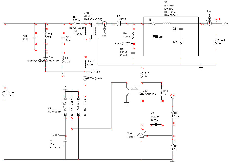
The NCP1050 through NCP1055 family of devices are monolithic high-voltage regulators, which enable end products to comply with low standby power requirements. The required converter functions are combined to allow a simple and economical power system solution for office automation, consumer and industrial products. A simplified working version of this circuit (See Figure 1) is contained within Intusoft’s ICAP/4 SPICE demonstration software. Look in Circuits\PowerDemo\ ON Semi Demo Templates\NCP105X Flyback.DWG. |
|||||||||||||||
 |
||||||||||||||||
 |
|
Figure 1. ON Semiconductor NCP105X Application Example.
An isolated Flyback example with NCP105X.
|
| A complete circuit drawing is also available as part of the demo that allows you to perform the following tasks using the ICAP/4 Windows Power Deluxe simulation package: If you own an ICAP/4 Windows Power Deluxe, ICAP/4 Professional,
Power Supply Designer or Test Designer package, and have a current maintenance
package, you can also download the complete circuit and required part
libraries from our web site. The NCP105X series is a Gated Oscillator
or hysteretic class Power Switching Regulator. Data sheets and application
notes can be found at Christophe P. Basso of ON Semiconductor describes the operation of this class of converters in his Switch-Mode Power Supply SPICE Cookbook. See http://www.intusoft.com/spicebook.htm. For data sheets, working templates and application notes on other converters and applications, see http://www.intusoft.com/pwrtemplates.htm. New models, created to evaluate the NCP1055, were placed into a single library (NCP105X.LIB) so that any version of ICAP/4 can be used to run the simulations for the wall adapter power supply. They include:
Aluminum Electrolytic Capacitor The model used for ceramic capacitors detailed in our January 2002 newsletter was modified with data supplied by UNITED-CHEMI_CON. The Aluminum Dielectric capacitors have higher low frequency DF than ceramic and the ESR at resonance can be estimated as Rmax = {(ESR/Cnom*33u+.03)/10}, where ESR is the 120 Hz ESR based on the data supplied. Tantalum Capacitor The tantalum capacitor model is slightly different because the capacitance changes with frequency. For other capacitors, the frequency sensitive parameter is dissipation factor, DF. To model both DF variations with frequency and capacitance variation, we combined an R-C ladder with the DF model used in other capacitors. Magnetic devices were modeled using Intusoft’s Magnetics
Designer. Magnetics Designer is normally used to design transformers and
inductors rather than analyzing them to get Spice models. Here’s how we
came up with Transformer For this design, the transformer is considered to belong to the inductor class since it is a Flyback device, transferring energy inductively. We’ll set up the design for maximum load for a low line input. This is usually a good starting point for Flyback designs because it runs the design at maximum duty ratio, assuring that we have a valid operating point for all line and load combinations. Here’s the data we need to enter: |
|||
| Core type:
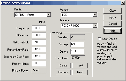
EI-TDK Ferrite Frequency: 100k Efficiency: 90% Ratio Isat/Ipk: 1.5 Primary Duty Ratio: .42 Secondary Duty Ratio: .42 Percent Ripple: 100 |
|||
|
Enter the voltage and DC load currents for each winding. Press “Insert” to add windings and Previous or Next to review the winding data. The core type we chose is closest to that specified in the application note. Frequency is given in the part data sheet. Efficiency is an estimate so that the input power is greater than the output power. The ratio of Isat/Ipk is used to guarantee that the device doesn’t saturate with up to 50% overload. If you set the percent ripple to 100%, then the turn on and turn off times can be independently varied as long as the sum is less than 100%. If you want to operate in continuous conduction mode (CCM), set the ripple to less than 100% and the secondary duty ratio will be set to 100 – primary duty ratio. Varying the primary and secondary duty ratios will cause the magnetizing inductance and the turns ratio to vary. The numbers were adjusted experimentally to agree with the design notes found in the application note and the test drawing. Run a simulation using “NCP105X Flyback.DWG” and input the duty ratios and loads measured in the simulations. When you get the correct data entry, press “Apply” and Magnetics Designer will give you a first cut design. The transformer described in the application note appears to have sandwiched the primary between a split secondary to lower the leakage inductance. In the inductor tab, select the secondary winding by left clicking in its Sector column. Then press the split button and use the << button to move the extra secondary winding to the first layer. Manually change the wire AWG of the first winding to match the last winding. Then increase the Insulation wrapper to 10m in. (254u m). The design now matches the specification, so switch to the IsSpice tab and adjust the artwork by selecting winding 1 as a secondary. Then press “Add to Library” and follow the instructions. You may want to edit the symbol so that the polarity is reversed for the secondary winding. To do this, select the entire secondary using the symbol editor, flip it and rotate twice and save the symbol using the name and library shown earlier. Conduct a test for all models you make. Drawing “uni10test.dwg” provides a test circuit to compare the simplified model with the complete model. You can see the ringing caused by adding the parasitic capacitance has changed the operation. Magnetics Designer’s Flyback SMPS Wizard is shown in Figure 2. |
|||
|
Figure 2. Flyback SMPS Wizard allows easy application
of design data.
|
|||
|
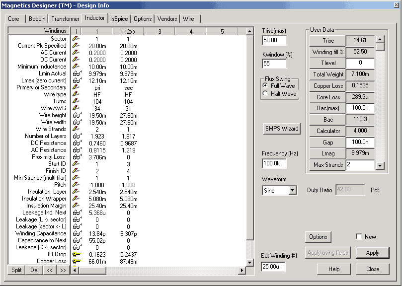
EMI Choke The EMI choke is a common mode filter wound in a manner that increases leakage inductance so that it acts as an effective normal (differential) mode filter as well. To make this design using Magnetics Designer it is necessary to set up 2 windings, each 10mhy on two sectors. This time we’ll start a new design and pick the core type from the core menu, “Toroid Ferrite”. Say yes to remove the bobbin, since toroids generally don’t have bobbins. The current Pk specified should be the common mode current (20m) while the AC and DC currents should be the value that causes heating in the winding(AC=DC=200m). Go to the bobbin tab and press Add Sector and then Auto Width. In the Inductor tab, for the second winding enter 2 for its sector column. Change the Kwindow to 55% so that there will be room for a shuttle to wind the toroid. Set frequency = 100k and Edt of winding 1 = 25u. This is the common mode volt-seconds to withstand; it goes along with Current PK Specified. You need to check to make sure these numbers aren’t exceeded in the simulation or else device saturation will occur. Finally, check “New” and press “Apply.” You can tweak your design manually and go through the same procedure as before to save it as a model. Magnetics Designer’s Flyback SMPS Wizard is shown in Figure 3. |
|||
|
Figure 3. Magnetics Designer’s Design Information
screen.
|
Intusoft is on the Move! |
In 1990, Intusoft moved from South Shores
to downtown San Pedro. Now we’re on the move again! Please note our new
address and phone: |
||
|
|
|
|
Amazin' Factoids |
||
| In 1986, Intusoft wrote what would become
its first of now 68 newsletters. That initial letter grew out of necessity,
as it explained fixes to a flawed Op-Amp model included in the company’s
first SPICE package. Since that time, the Intusoft Newsletter has expanded
to include much more than bare-bones application notes. It has mushroomed
into a virtual information goldmine on every aspect of circuit simulation
and modeling with over 1,300 articles written to date. |
||
| Newsletter Resources
• Access over 24 different articles on behavioral modeling alone, including building accurate models of differentiators, electric motors, gears, multipliers, servos and other mechanical systems. • Creating and plot black-body radiation curves with step-by-step instructions. • Get information on modeling 14 different capacitor types. • Read 20 articles on filter design. |
||
| The newsletter itself is free. But, as a subscriber, you receive actual working circuits and models described within each newsletter and a host of new models unavailable to those who do not subscribe. The cost of a Domestic U.S. subscription is currently $40 per year.Take a look at the Newsletter Index. It is your on-line guide to circuit simulation. It is available at no cost as a resource to make your design and test job easier! |
||
Starting Designs Using Simulation |
||
There has been much discussion about
simulation versus breadboards or prototypes. It’s really a mistake to
pit one against the other. As good as your simulation might be, you may
have overlooked an important aspect of the design that prevents production
hardware from working. On the other hand, a prototype could be working
because of a lucky combination of part tolerances and the design could
have a terrible time in production.
Simulation is an adjunct to both analysis and design. The power of simulation in the design phase is to try out concepts using components that may not be available for weeks or even months. Analysis by simulation replaces simplified mathematical descriptions with more exact numerical analysis. Simulators routinely solve nonlinear equation involving thousands of simultaneous equations; clearly an impossible task using classical pencil and paper approaches. With Intusoft’s simulation templates, the design of switch mode power electronics using simulation becomes the preferred way to try out new design ideas. Here are some of the things you can do: |
||
| |
|
|
Nearly everything you need to know can
be predicted using simulation. We look at huge digital IC’s and wonder
why power circuitry can’t be produced without prototyping. But this overlooks
the fact that the digital designers don’t sell their first Silicon. They
test it and make modifications based on those tests. The discrepancy between
simulation results and actual hardware behavior is resolved by tweaking
the simulation model.
Over time, the IsSpice simulator has gotten better as have the models. Power electronic models are now routinely made for both switching and average behavior. The large signal average models run up to one thousand times faster than switching models so that you can “center” your design using an Optimizer. Design centering gets the most out of a design by using just the right part values to get the best production yield and performance. |
||
Power System Models |
||
When designing a power supply, the interaction
with the mains delivering power and loads consuming the regulated power
is often overlooked. Designing power supplies for test sets that supply
raw power, for example simulating an avionics battery, can be quite a
challenge. What should be done when the combination oscillates or produces
unusual line harmonics? Perhaps the best answer is a decent simulation
that exposes these problems before the system is put together. You may
not know the details of either the mains or the load, however, there are
some educated guesses that may expose system interactions.
First, the designer should know whether or not the load is a “constant power” device (Switching Regulator) and whether or not AC loads are present, for example, 400Hz motors or gyros. From the line perspective, you can examine the power distribution system in the application and test environments. The system must work in its test environment as well as the final field environment. |
||
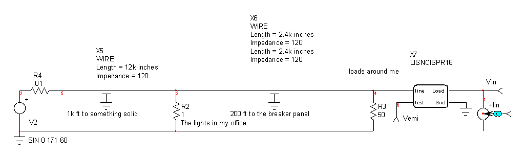 |
|
Figure 4. Mains simulated using transmission lines.
|
|
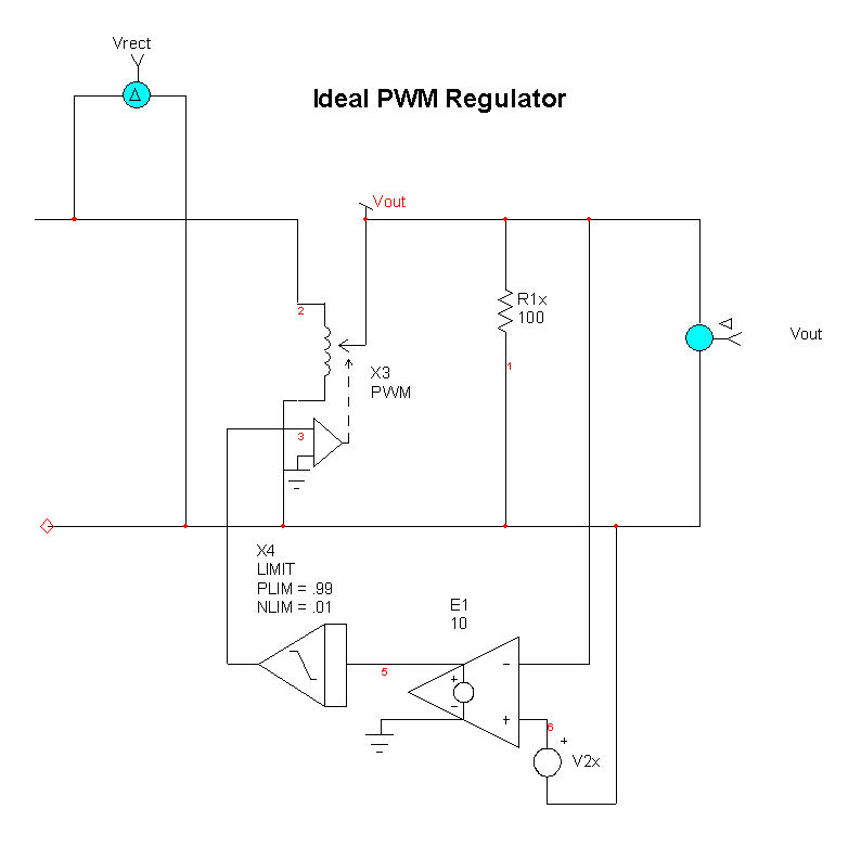
Figure 4 shows a transmission line model of a typical Office/Laboratory. The transmission lines have been replaced with lumped R-L-C models to gain simulation efficiency at lower frequency, or for long simulation time spans. On the load side, we can assume that a broadband pulse width modulator model will expose a “worst case” negative resistance load by using the model shown in Figure 5. |
|
Figure 5. An ideal pulse width modulator using a
broadband model provides constant power load.
|
The broadband PWM model is made by using a ideal
“transformer” that conserves the input and output power relationship and
uses a fixed gain regulator to provide constant voltage output into a
resistive load. The PWM controller has a limited duty ratio to avoid singularities
with zero input voltage or zero input current cases.
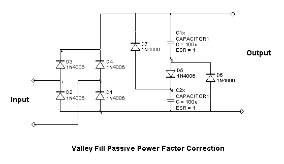
After that, a DC and AC load can be simulated. The AC load will reflect back through the test set power supply to the mains. Then, using the Intusoft power supply template models, you can explore the interaction of the line and loads on your power supply performance. An example of applying the system model to a real circuit is illustrated in Figure 6 with the “passive” Valley Fill circuit proposed by Jim Spangler [1]. While it works nicely with fluorescent lamps, it would be interesting to see what happens with a constant power load and simulated power line. |
|
|
| Figure 6. Valley Fill Passive Factor Correction
|
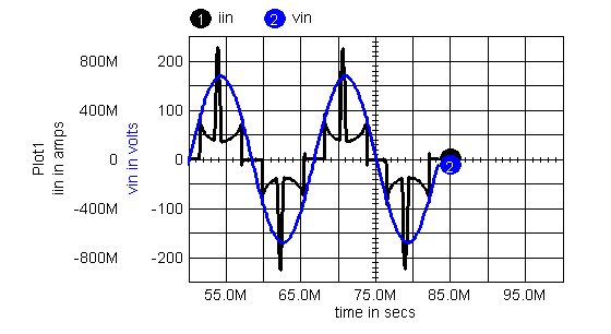
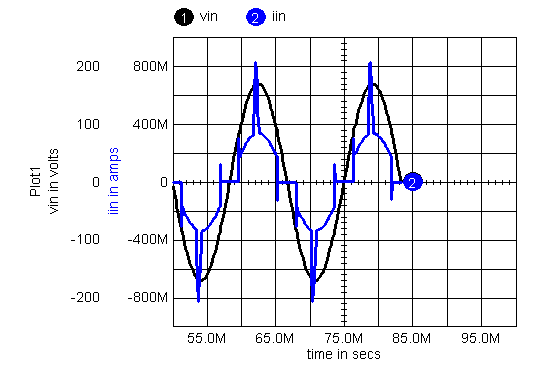
| Figures 7 and 8 show the results with and without the constant power load. Unfortunately, the simulated PWM regulator makes the Valley Fill less effective as a power factor correction technique. You can also measure the Vemi voltage and use the emi script to check out CISPR16 compliance. |
||
| Figure 7. Constant Power Load; PF
= 80.6, THD = 72.4% |
||
| Figure 8. Resistive Load; PF = 91.7,
THD = 42.8% |
||
| References: [1] Valley Fill Passive Power Factor Correction, Jim
Spangler and Anup K. Behara APEC |
||
| Back in June of 2000, we introduced a new time step control option, VSECTOL. See Newsletter 60. Circuits that switch states behaviorally won’t interact with the IsSpice time step control algorithms. VSECTOL solves this problem by reducing the time step to maintain volt-second accuracy. This algorithm allows a much large MAXSTEP setting in the .TRAN control statement. |
||
Originally, VSECTOL
only checked the main circuit nodes. We subsequently included subcircuit
nodes to the test. The way it works is for the simulator to take the absolute
value difference of the predicted node voltage and the calculated node
voltage and multiply the result by the time step. When the product is
greater than the VSECTOL option, the time step is decreased. Hysteresis
is used in the algorithm, to keep the time step from jumping back and
forth. Here are some things to do when using VSECTOL to control the time
step: |
||
|
||
| Low voltage models for oscillators, logic gates and comparators are frequently used in the underlying macro models. To give these models the same weight as the higher voltage main circuit switches, its necessary to create dummy nodes that transform the voltage to a comparable value. Here’s an example of a behavioral inverter: |
||
|
||
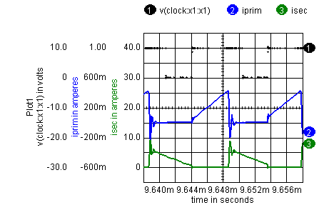
| bvsectol and rbvsectol were added to increase the VSECTOL sensitivity. Figure 9 shows the time step varying over one cycle of a Flyback Regulator simulation. The clock, shown in waveform 1 steps its transition down to under 15nSec rise and fall times and expands to about 1.5uSec when there is no switching activity. Notice the finer switching resolution near the Flyback interval near the center of the screen. |
||
| Figure
9. Variable time step control places computational power where it’s needed. |
||
Similarly,
you can add B elements to make voltage nodes out of branch currents so
that critical currents can also take advantage of the VSECTOL option.
The diode current of D1 can be used as follows:
BD1 100 0 v=1k*I(D1) RBD1 100 0 1k
|
||
Unfortunately,
the diode equation is temperature dependant and low emission coefficients
create numerical overflows when circuit temperature is changed even slightly.
In IsSpice, the global circuit temperature of a diode can be overridden
using the Temp=27 instance parameter. So when you use diodes with low
emission coefficients, set Temp=27 in the diodes instance parameters and
you will be able to vary circuit temperature and have your diode act as
a nearly ideal switch. |
||
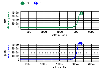
| Figure
10. Low emission coefficient diodes are nearly ideal, conducting current
at lower voltage. |
||
Transit TimeThe transit time; TT for diodes and TF and TR for BJT’s,
affect device storage time. The behavior of these models is to produce
a snap recovery; that is, the device switches instantly from ON to OFF.
Soft recovery diodes are modeled using macro modeling techniques and use
more simulation resources. If you need a diode or BJT to be used as a
behavioral switch, then you do not need to specify a value for transit
time. It’s usually a good idea to give the device a reasonable value for
capacitance (CJO for diodes) so that the ringing from inductive load switching
doesn’t become infinite. Using gear integration also resolves the issue
of zero capacitance inductive switching. |
||