
|
|
|
| Newsletter List | |
|
|
General Feedback Theorem (GFT) |
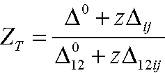
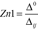
| Dr. R. David Middlebrook with the California Institute of Technology developed the theorem, which describes a control system in terms of its response to signal injection inside the control loop. Application of the GFT provides simulation techniques for measuring control system characteristics when the loop is closed. Of particular interest is the loop gain and its contribution to system stability using Bode Plots. With the loop closed, the simulator automatically accounts for the DC operating point and circuit loading is properly handled at the signal injection point. The generalization of this technique removes the previous restriction of the single injection method described in Newsletter 57. Back in the days before computer simulation, network equations were commonly solved using determinants. Interestingly, determinants provide insight for understanding the effect of one network element on the overall network behavior. For example, the following equation taken from Bode in 1945 [1] shows how impedance, z, somewhere in a network affects the transfer impedance, ZT, between the network input current at node 1 and output voltage at node 2 with an impedance z belonging to Zij in the original determinant. |
|
||||||||||||||||
where the superscript,
This comes
about by expanding the determinants and their minor elements into the
parts shown in (1a). The terms
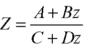
This representation is a bilinear transform that maps variations in z at each frequency into circles in Z. Re-arranging Bodes equation results in the following interpretation.
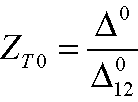
Where ZT is the impedance with z present
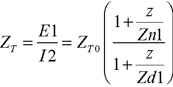
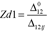
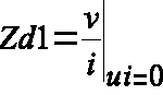
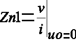
Now we can further generalize the concept to measure the transfer response of any pair of voltages or currents, using the notation ui for input voltage or current and uo for output voltage or current. With this interpretation, this becomes the Extra Element Theorem [2]. Middlebrook goes on to show that:
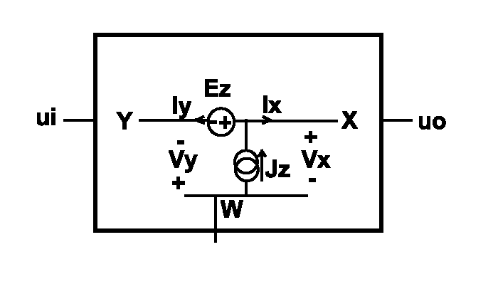
Where v and i are the voltage and current in z. Both Zn1 and Zd1 can be measured using a simulator by injecting a voltage in place of z and measuring the ratio of v/i. For Zd1, the input, ui, is set to zero. However, to calculate Zn1 you must null uo and not set it to zero. The null is achieved by connecting a high gain amplifier between uo and ui. The rational for this null injection technique was discussed in the last newsletter, NL69. Moreover, we can replace Z with voltage or current sources so that we are dealing with the response of a network transfer function to signals injected at some point in the network. Next, we can expand the EET to the 2EET by considering 2 extra elements. Dr. Middlebrook details this expansion in [3] and shows how it can be used in [4]. Using dual voltage and current injection, the GFT is capable of having a loop-cut or injection point in the middle of a network where the input is neither a current source or a voltage source. Applying the EET twice, once for each source or by directly using the 2EET, exposes an extra product term as shown in (8). |
| Using the voltage and current definitions in Figure 1, the loop gain T is given by equation 8.
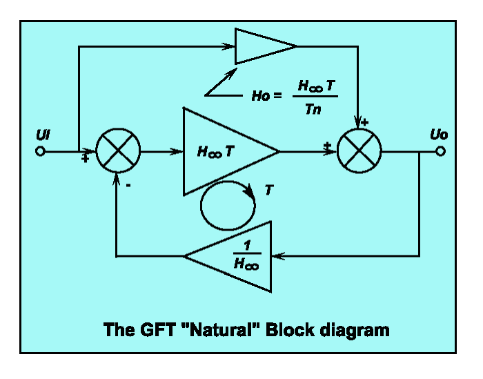
Finding T, then requires 3 simulations. The GFT is more than just a method to extract the principal loop gain. It reorganizes control system theory, providing a new set of parameters used for design-oriented analysis. Beginning with a control system block diagram shown in Figure2, |
||
|
Figure 2. The GFT “Natural” Block diagram |
||
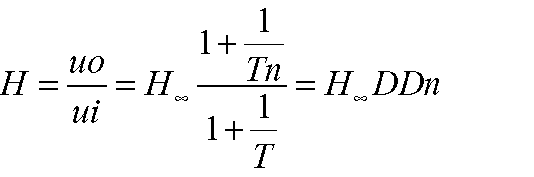
Notice the
relationship between the formulation in (9) and (2). That’s how the EET
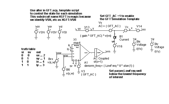
gets to be part of the GFT. The term H Implementing the GFT in ICAP/4 The GFT has been implemented using ICAP/4’s powerful simulation templates. The GFT models include analog multiplexers that are configured by the template scripts to change the way stimulus and nulling amplifiers are connected. After the null signal is selected, it goes through a high pass filter so that the DC bias is not altered. Finally, a high gain is applied in order to make the null target vanishingly small. Up to 13 simulations
are needed to get the complete GFT data set. Figure 3 illustrates how
the GFT model selects the signals to be nulled using an analog multiplexer.
The null selections are made using the ICL Alter command shown in Table
1. The Script must know the name of the subcircuit so the GFT subcircuit
must be named Xgft. A new ICL function, msgbox, is used to notify the
user if he forgets this requirement. |
||
|
Figure 3. The various nulls are selected using a behavioral analog multiplexer, controlled using Alter commands in the template script. |
||
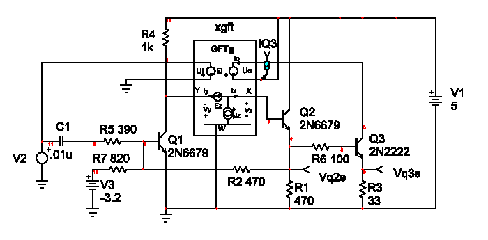
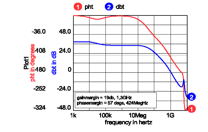
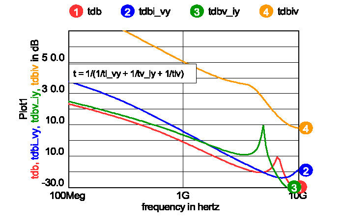
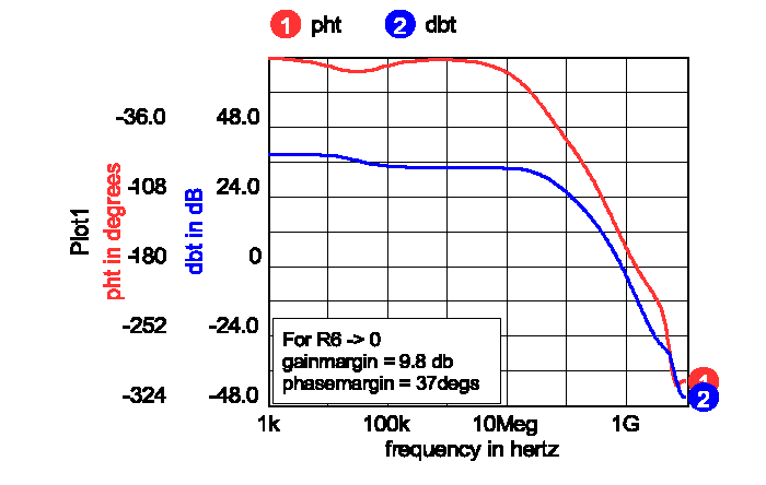
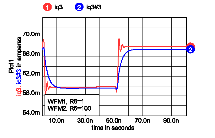
More information is available when the input and output are included. Figure 4 illustrates the technique used for the GFTg model and a portion of the template script. Several built-in scope scripts can be invoked to plot some common functions. For example, running “gft/T” will make a Bode Plot of the principal loop gain, T as seen in Figure 5. While the math behind the GFT can be daunting, its use is simple. The transistor amplifier shown in Figure 4 illustrates the use of the GFT in exploring this design. This is a portion of Sample.dwg, a drawing delivered with ICAP/4 that is used for training. Q1 and Q2 have been upgraded to use wider bandwidth transistors, which requires the addition of R6 to eliminate ringing. Breaking the loop at Q2’s base lets us look at the Bode plot, shown in figure 5. The 3 components of the loop gain T are shown in Figure 6. Figure 4. Transistor Amplifier with feedback Figure 5. The GFT principal loop gain. Figure 6. The principal loop gain and its components Figure 7. Bode plot with small R6. Figure 8. Increasing R6 damps the ringing as confirmed by the GFT analysis. [1]
H.W.Bode, “Network Analyais and Feedback Amplifier Design”Princeton, NJ:
Van’Nostrand, p. 10, 1945. |
| EDIF
Capability Coming Coming soon is a Layout and Auto Routing package. We’ll let you know as we fill in the details. Connect
Current Test Point to Subcircuit Pins
The subcircuit test point creates a voltage source and an extra node to measure the current. The new test point is saved into the new file version. Saving to a file version older than version 13 will delete the test points. Test
Point Support Added to B-Elements IntuScope
Now Reads in CSDF File Format Successfully
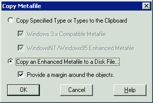
Reduce Schematic Image for Publication Save
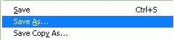
Schematic Image Directly to EMF File Figure 9. Save directly to EMF file instead of to the clipboard. You can also save Enhanced Metafiles to disk. The EMF format is the preferred Windows clipboard format. It saves drawings and graphs as vectors so that you can render to the precision of your output device. “Save as” added to SpiceNet File Menu
Figure 10. New Save as... command “Save as…” has been added to the SpiceNet file menu, adding to the existing “Save Copy as…” The difference between the two is that “Save as…” abandons the current drawing and saves changes in the new “Save as…” file. It then switches the project to this new file. “Save Copy as…” works as before to produce a back up copy, but retains the current drawing as active. This adds to recent capability that enables projects to automatically switch to the drawing that the user desires as active, ultimately to invoke simulation control and running simulation. XML
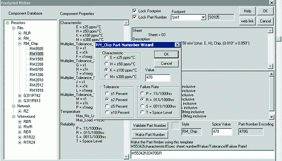
Database for PCB Footprints Figure 11. New Footprint Picker builds part numbers and selects package footprints The xml files are named ??.type, where ? is the spice key for the part. For a resistor, the database is RR.type. We have initiated databases for resistors, capacitors and inductors using the NASA Parts Selection List, NPSL: The list is comprehensive, and generally parts are also available to commercial specification. We’ve added built in parsers to help build the part number as shown in Figure 11. User DLL’s can be added to augment or replace the built-in parsers. The benefit of this feature is that it makes it even easier to be able to export PCB netlist with the correct syntax. Intusoft currently supports PCB netlist export to any package that can read in the following formats. Tango PWB - Netlist for Accel New
XP Style UI |
 |
Figure
12. SpiceNet and IntuScope now support the
|
|
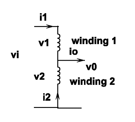
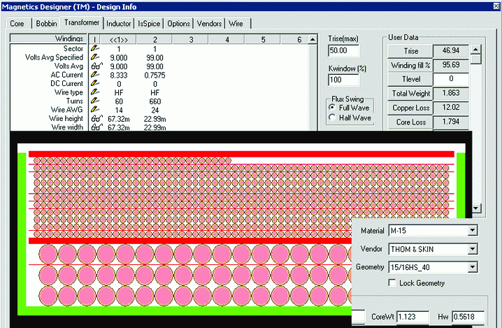
An auto transformer, shown in Figure 13, is a 2-winding transformer connected so that its windings are in series. Magnetics Designer needs as its input the voltage and current for each of these windings. If the design requirement calls for a prescribed output current, with a transformer ratio vo/vi, then,
K is a waveform shape factor, so for sine waves,
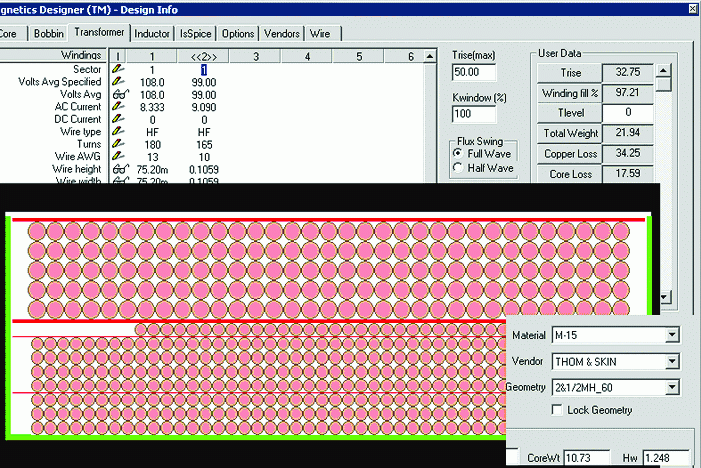
Figure 13. As v1 approaches 0, the power handled by the transformer action approaches 0. Autotransformers sacrifice isolation for extremely high efficiency when the turns ratio is near unity. Figure 14 shows the results of a Magnetic Designer design of an isolation transformer going from 120 VRMS to 110VRMS at 1KW. Figure 15 meets the same requirements but uses the autotransformer configuration.
Figure 14: A 1KW isolation transformer Figure 15: A 1KW autotransformer
Magnetics Designer
picked the “best” geometry from a set of rectangular laminations with
variable stack size. The stack height to width ratio was .789 for the
autotransformer and .444 for the isolation transformer. The automatic
design algorithm searches cores from the smallest power handling capability
to the largest, beginning with the theoretically smallest core. Trial
designs are made and discarded if the temperature rise is above the specification.
Several “larger” power capacity designs are tested to see if they produce
a lower weight. The lowest weight design is then presented to the user.
The user is free to lock in any core, thereby disabling the automatic
core selection. For each core, Magnetics Designer makes trial windings
to pick the wire size under the constraint of minimum temperature rise.
For low frequency designs like this example, the winding area will be
nearly 100% full. On the other hand, high frequency designs will have
significant losses because of the skin effect, proximity loss, and in
some cases gap induced eddy currents. Magnetics Designer builds on the
work of Bennet and Larson [5] to predict these losses.
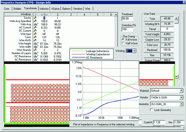
Figure 16 shows what happens to the isolation
transformer if the frequency is increased to 1KHz using 4mil laminations. Figure 16. High frequency losses increase sharply for windings in the center of the stack where the field is highest. There is a sharp increase in Rac in the 1KHz to 10Khz region due to the skin effect. The result is to cause the “best” design to under-fill the window. Interestingly, the onset of these high frequency effects occurs at lower frequencies as the power level increases. [5] Bennett and Larson, Effective Resistance to Alternating Currents of Multilayer Windings, AIEE Transactions 1940, vol. 59, pages 1010-1017. |
||||||||||||||||||||||